Facilities
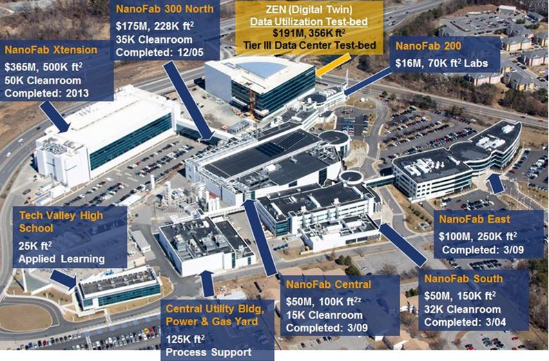

The AMP Center provides access to the CNSE’s Albany Complex including:
- New York-Power Electronics Manufacturing Consortia (NY-PEMC) facility
- Zero Energy Nano (ZEN) facility
- NanoFab 200 facility
- NanoFab 300 facilities
New York-Power Electronics Manufacturing Consortia (NY-PEMC)
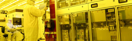
NY-PEMC is a public-private partnership producing the next generation of power electronics at Colleges of Nanoscale Science and Engineering 150 mm SiC fab. CNSE’s world-class research and development resources, with the expertise of consortia members, will drive tremendous advances for businesses, the power electronics technology and academic communities. http://ny-pemc.org/
Zero Energy Nanotechnology (ZEN)
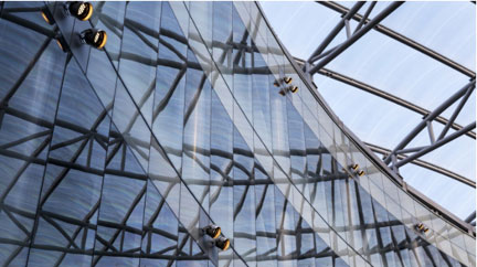
The Zero Energy Nanotechnology (ZEN) facility, completed in 2015, is CNSE’s most recent expansion project, a 356,000-square-foot facility that serves as a living laboratory for cyber-physical systems.
NanoFab 200
NanoFab 200 was completed in June 1997. This 70,000 square foot facility includes 4,000 square feet of cleanroom space, plus CNSE’s metrology labs and office space for programs.
NanoFab 300 facilities:
 NanoFab 300 North
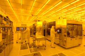
NanoFab 300 North is a 228,000 square foot, $175 million facility including 35,000 square feet of cleanroom space with Class 1 capable 300mm wafer production. The NFN facility also houses the world’s first extreme ultraviolet (“EUV”) Alpha Demo Tool, developed by ASML.
NanoFab 300 South
NanoFab 300 South, completed in March 2004, is a 150,000 square foot, $50 million facility including 32,000 square feet of cleanroom space. The facility also includes classrooms and offices for the College of Nanoscale Science and Engineering.
NanoFab 300 East was completed in 2009. The 250,000 square foot, $150 million facility includes 15,000 square feet of 300mm wafer, class 1 capable cleanroom space. The nanofabrication complex houses the latest nanofabrication technology available, and house all the technology and equipment needed for the proposed project including resist spinners, UV immersion steppers, nanoimprint lithography, EUV lithography, E-beam lithography, PVD, CVD, PECVD and ALD deposition tools, reactive ion etching, acid/base and solvent fume hoods.